|
USRP Hardware Driver and USRP Manual
Version: 4.6.0.0-7-gece7c4811
UHD and USRP Manual
|


|
|
USRP Hardware Driver and USRP Manual
Version: 4.6.0.0-7-gece7c4811
UHD and USRP Manual
|
|
The FBX daughterboard is a four-channel, balun-coupled transceiver board.
The FBX daughterboard is the daughterboard for the Ettus USRP X440.
Feature list:
See the RF section in the Ettus USRP X440 Specifications for a comprehensive FBX daughterboard specifications list.
The FBX daughterboard has four independent transceiver chains. The following simplified block diagram shows the structure of a single chain:
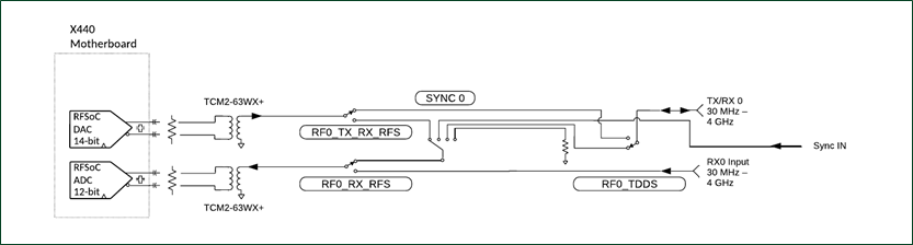
It is a balun-coupled transceiver, with symmetric TX and RX path. The FBX is a passive design, with no gain or filter stages and complements the direct IF sampling design of the X440. Compared to most other Ettus USRPs this requires consideration of the utilized Nyquist zone and resulting aliasing effects. As a result, most applications will require external filters or signal conditioning. UHD provides help coordinating the control of such front ends in the form of the Extension Framework documentation.
One property of this design is that signal aliases need to be considered. On the ADC all observed alias tones are actually the same frequency but the RFDC cannot distinguish the incoming frequencies. In contrast, the DAC will send out all alias frequencies at once. Signal aliases will occur in each Nyquist zone and appear as mirrored signal tones around multiples of half the converter rate (Fc/2). The first Nyquist zone (N1) is defined as the frequency range between 0 and Fs/2, and the second Nyquist zone (N2) stretches from Fs/2 to Fs. Other Nyquist zones are defined in ascending order, each extending Fs/2. The following diagrams illustrate the Nyquist zones and tone aliases for select converter rates (Fc). Note that the diagrams do not show that the achievable passband within a Nyquist zone gets smaller the higher the Nyquist zone order. The passband in lower Nyquist zones can be roughly calculated as 0.4 * Fc.
Nyquist Zone example with Converter Rate = 1GS/s
Nyquist Zone example with Converter Rate = 4GS/s
Applications should prefer converter rates that can contain the desired signal spectrum in a single Nyquist zone, or split the signal spectrum among multiple channels and devices. For details about the relationship between converter rate (Fc) and IQ sample rate (Fs) refer to Master Clock Rates.
The Xilinx RFDC used in the X440 consists of an integrated design that interleaves multiple converters to realize the high RF-ADC rates. In this design an RF-ADC consists of 8 interleaved sub-ADCs. The resulting interleaved spurs are minimized by the integrated self-calibration executed by UHD. For details on controlling the self calibration execution refer to ADC self calibration.
All switches on the FBX are controlled via registers that are exposed as a subset of the Radio RFNoC block register space (starting at address 0x80000). The design differentiates between switches that are directly controlled by the FPGA and support fast switching times, and ones that the FPGA controls via an I/O expander.
The first kind are the switches referenced by the UHD driver as RF switches (e.g. RFx_TDDS, RFx_RX_RFS, RFx_TX_RX_RFS). These can also be controlled via ATR states (see also Auto-Transmit-Receive Registers (ATR)).
The second kind are the SYNC_CTRL switches. Use of the I/O expander makes their operation slower and requires readbacks from the I/O expander. For that reason they are at the utmost set when an antenna setting is changed, and their position is unaffected by ATR state changes. These switches are intended to connect signal chains to optional synchronization signals, that UHD may support in a future release.
The FBX has two MMPX ports per channel, called "TX/RX0" and "RX1". In addition, the antenna values can be set to "CAL_LOOPBACK" to loop back the Tx path into the Rx path (this is sometimes required for calibration purposes). The Rx antenna value can also be set to "TERMINATION" to terminate the Rx path.
Use the uhd::usrp::multi_usrp::get_rx_antennas() or uhd::usrp::multi_usrp::get_tx_antennas() API calls to enumerate the valid antenna names. When using RFNoC API, use the uhd::rfnoc::radio_control::get_rx_antennas() and uhd::rfnoc::radio_control::get_tx_antennas() calls, respectively.
Additionally, the FBX has a single MMPX port, called SYNC IN. This input is intended to route an optional synchronization signal to the signal chains, and may be supported by UHD in a future release (see also SYNC_CTRL switches in Digital Control).
The FBX daughterboard is equipped with two LEDs per channel, one for "TX/RX0" and one for "RX1". These LEDs behave as follows:
| LED State | TX/RX0 | RX1 |
|---|---|---|
| Off | Port is inactive | Port is inactive |
| Green | Port is receiving | Port is receiving |
| Red | Port is transmitting | N/A |
Every channel has one "locked" sensor for the LO stages (nco_locked). A "virtual" sensor called lo_locked confirms that the LOs that are currently engaged are locked. The "NCO lock" sensor is not on the daughterboard (it is part of the RFSoC FPGA), but to simplify the API it was categorized like typical LO lock sensors. The NCO "unlock" state is not used to signify a loss of reference lock, but to signal that the NCO is still in reset.
Additionally, the FBX has a temperature sensor: temperature. While the UHD API allows addressing a sensor based on direction (RX/TX) and channel (0/1/2/3), there is only one physical temperature sensor, and it will return the same value regardless of which channel or direction is selected.
The following API calls can be used to enumerate available sensors, and query their values:
Like other USRPs, the X440 provides GPIOs to the daughterboards that communicate the RX/TX state. The FBX is, by default, configured to switch settings based on the current state (RX, TX, full duplex, idle). For example, the TX/RX antenna is switched between the TX and RX channels depending on the state.
Example: Assume the device is transmitting, but not receiving, on channel 0. The FPGA will set the ATR pins for channel 0 to a binary value of 0b10, which equals a decimal value of 2. This mode of using the ATR pins is called the "classic ATR" mode and is the default behavior. UHD currently supports configuring channel 0 and 1 as ATR sources for GPIO pins.
The FBX daughterboard provides one additional mode of utilizing those pins:
Note that combining the "FPGA controlled" mode on one channel with the "classic" mode on the other channel would yield a possibly conflicting configuration.
Usage of these modes is considered highly advanced usage of FBX. The "FPGA controlled" mode is not supported by UHD without custom modifications (it is possible, however, to manually write to the appropriate registers to use this mode). Using this mode would also require modifications of the FPGA image to add custom controls to the ATR GPIO pins.
 1.8.13