|
USRP Hardware Driver and Device Manual
Version: 4.10.0.0-0-g2af4ddb9
UHD and USRP Manual
|


|
|
USRP Hardware Driver and Device Manual
Version: 4.10.0.0-0-g2af4ddb9
UHD and USRP Manual
|
|
The X4x0 series of USRPs comes in three variants: The USRP X410, the USRP X420, and the USRP X440. All three variants share the same enclosure and motherboard, and are collectively referred to as X4x0.
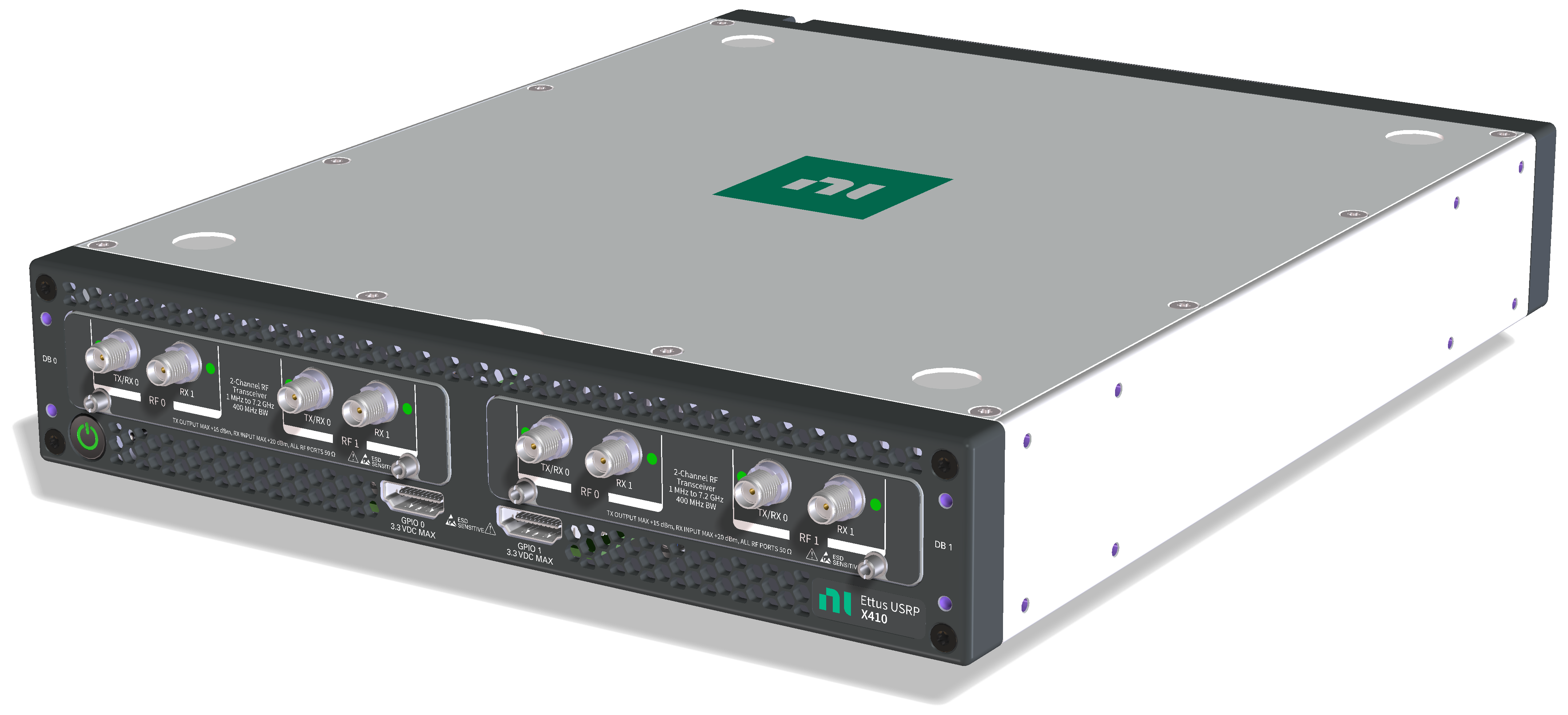
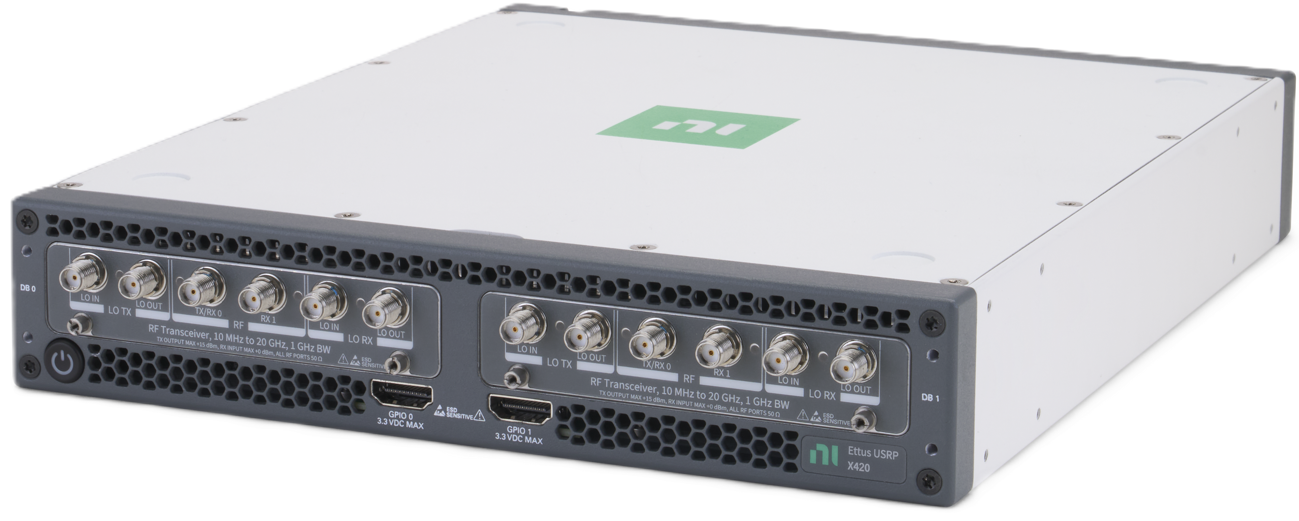
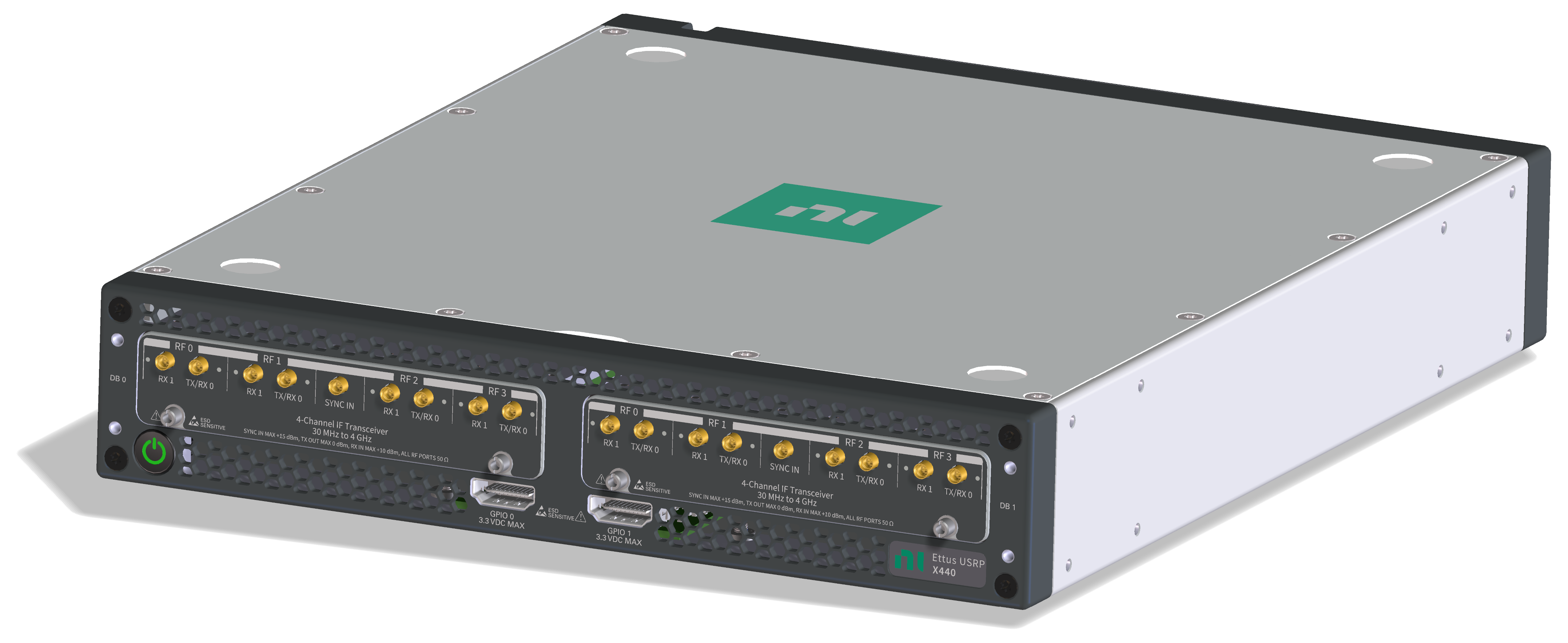
The Ettus USRP X4x0 is a fourth-generation Software Defined Radio (SDR) out of the USRP family of SDRs. Depending on the variant, it contains either two ZBX Daughterboards for a total of 4 channels at up to 400 MHz of analog bandwidth each, two HBX Daughterboards for a total of 2 channels at up to 1000 MHz of analog bandwidth each, or two FBX Daughterboards for a total of 8 channels at up to 1.6 GHz of analog bandwidth. The analog features of the ZBX Daughterboard, HBX Daughterboard, and the FBX Daughterboard are described in a separate manual page.
The USRP X4x0 features a Xilinx RFSoC, running an embedded Linux system. Like other USRPs, it is addressable through a 1 GbE RJ45 connector, which allows full access to the embedded Linux system, as well as data streaming at low rates. In addition, it features two QSFP28 connectors, which allow for up to 4x10 GbE or 1x100 GbE connections each. The RFSoC used on the USRP X410 and USRP X420 is a ZU28DR speed grade 1, on the USRP X440 the ZU28DR speed grade 2.
The front panel provides access to the RF connectors (SMA for X410 and X420, MMPX for X440), Tx/RX LO input and output connectors (SMA, X420 only), Tx/Rx status LEDs, programmable GPIOs, and the power button. The rear panel is where the power and data connections go (Ethernet, USB) as well as time/clock reference signals and GPS antenna.
The main chip (the SoC) of the X4x0 is a Xilinx Zynq UltraScale+ RFSoC (ZU28DR). It contains an ARM quad-core Cortex A53 CPU (referred to as the "APU"), an UltraScale+ FPGA including peripherals such as built-in data converters and SD-FEC cores, and an ARM Cortex-R5F real-time processor (the "RPU").
The programmable logic (PL, or FPGA) section of the SoC is responsible for handling all sampling data, the high-speed network connections, and any other high-speed utilities such as custom RFNoC logic. The processing system (PS, or CPU) is running a custom-built OpenEmbedded-based Linux operating system. The OS is responsible for all the device and peripheral management, such as running MPM, configuring the network interfaces, running local UHD sessions, etc.
The programmable logic bitfile contains certain hard-coded configurations of the hardware, such as what type of connectivity the QSFP28 ports use, and how the RF data converters are configured. That means to change the QSFP28 from a 10 GbE to a 100 GbE connection requires changing out the bitfile, as well as when reconfiguring the data converters for different master clock rates. See FPGA Image Flavors for more information.
It is possible to connect to the host OS either via SSH or serial console (see sections SSH Connection and Serial Connection, respectively).
The X4x0 has a higher maximum analog bandwidth than previous USRPs. The USRP X410 can provide rates up to 500 Msps, resulting in a usable analog bandwidth of up to 400 MHz.
The USRP X420 can, depending on the FPGA image used, provide up to 1250 Msps of sampling rate, resulting in a usable analog bandwidth of up to 1 GHz on two channels.
The USRP X440 can, depending on the FPGA image used, provide up to 2048 Msps of sampling rate, resulting in a usable analog bandwidth of up to 1.6 GHz on two channels, or 8 channels at 500 Msps.
In order to facilitate the higher bandwidth, UHD may use a technology called Data Plane Development Kit (DPDK). See the DPDK page for details on how it can improve streaming, and how to use it.
The Ettus USRP X410 contains two ZBX daughterboards. To find out more about the capabilities of these analog front-end cards, see ZBX Daughterboard.
The Ettus USRP X420 contains two HBX daughterboards. To find out more about the capabilities of these analog front-end cards, see HBX Daughterboard.
The Ettus USRP X440 contains two FBX daughterboards. Unlike the ZBX and HBX daughterboards, they have no analog mixers or filters, but directly connect the converters to the RF connectors. To find out more about the capabilities of these analog front-end cards, see FBX Daughterboard.
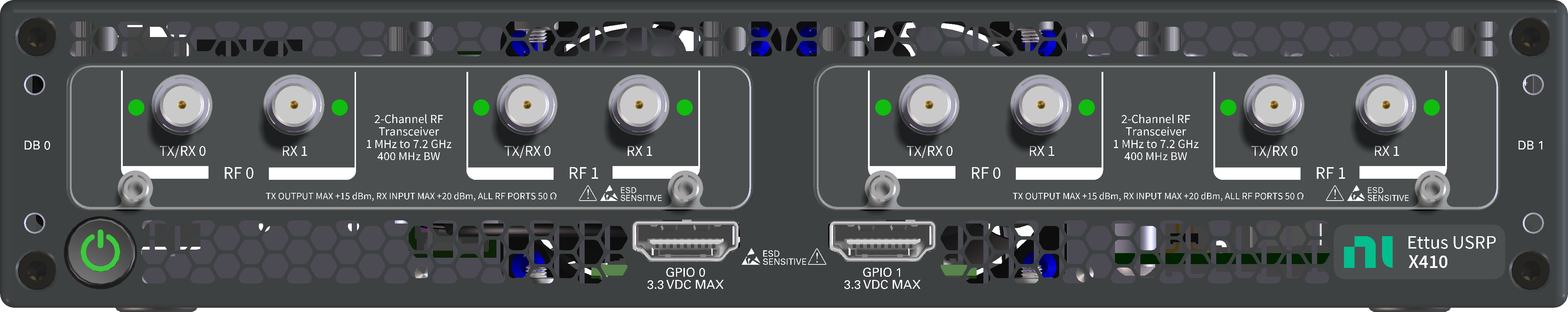
The X410 front panel provides access to the RF ports and status LEDs of the ZBX Daughterboard. It also provides access to the front-panel GPIO connectors (2x HDMI) and the power button.
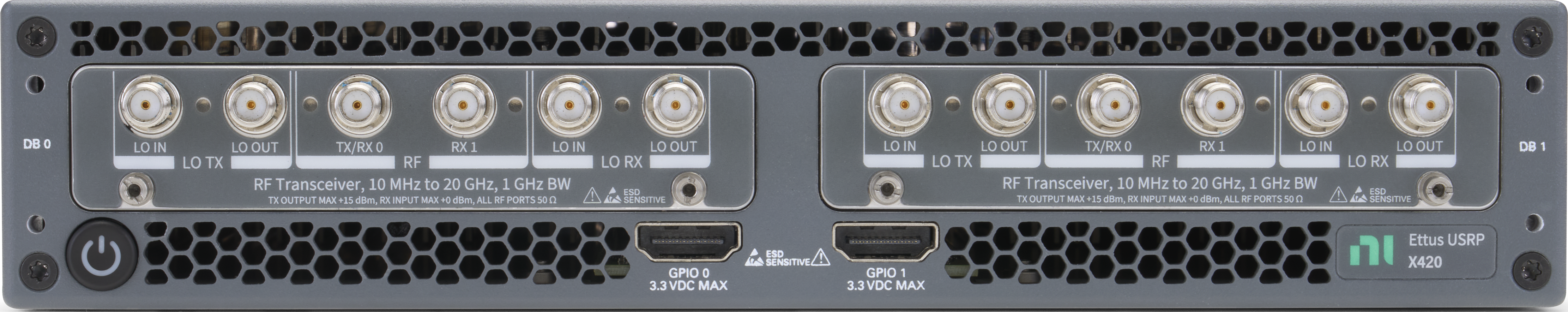
The X420 front panel provides access to the RF ports, LO ports and status LEDs of the HBX Daughterboard. It also provides access to the front-panel GPIO connectors (2x HDMI) and the power button.
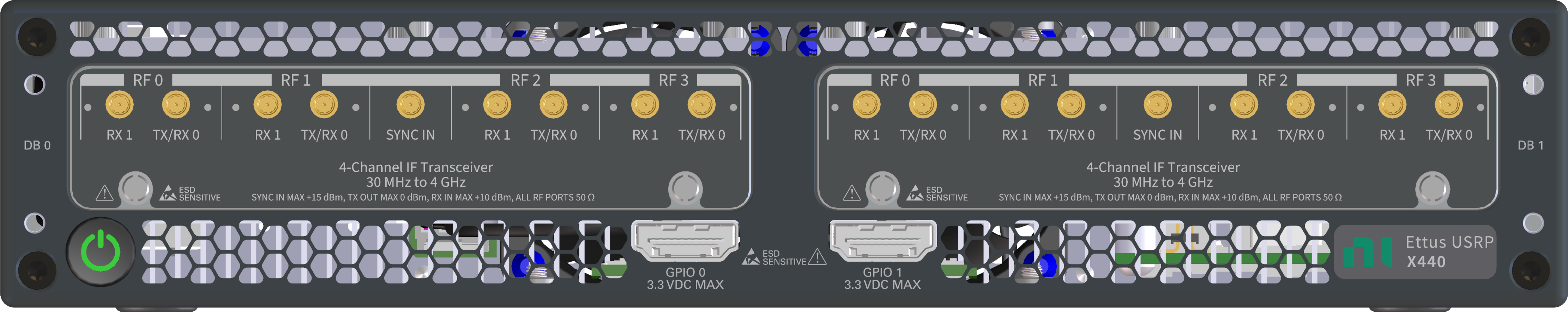
The X440 front panel provides access to the RF ports and status LEDs of the FBX Daughterboard. It also provides access to the front-panel GPIO connectors (2x HDMI) and the power button.
The SYNC IN connectors provide access to additional circuitry for advanced time synchronization, in the current version of UHD, they are not supported.
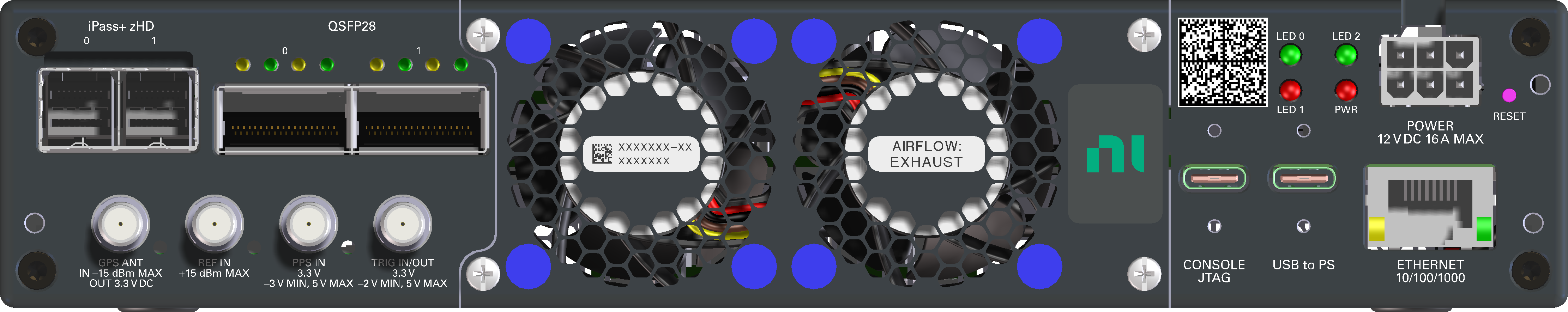
The back panel provides access to power, data connections, clocking and timing related connections, and some status LEDs:
The back panel is identical between X4x0 variants.
The X4x0's cooling system uses a field replaceable fan assembly and supports two variants: one that pulls air front-to-back and one that pulls air back-to-front. By default, the unit comes with the front-to-back fan assembly.
The STM32 microcontroller (also referred to as the "SCU") controls various low-level features of the X4x0 series motherboard: It controls the power sequencing, reads out fan speeds and some of the temperature sensors. It is connected to the RFSoC via an I2C bus. It is running software based on Chromium EC.
It is possible to log into the STM32 using the serial interface (see Connecting to the Microcontroller). This will allow certain low-level controls, such as remote power cycling should the CPU have become unresponsive for whatever reason.
The main non-volatile storage of the USRP is a 32 GB eMMC storage*. This storage can be made accessible as a USB Mass Storage device through the USB-OTG connector on the back panel.
The entire root file system (Linux kernel, libraries) and any user data are stored on the eMMC. It is partitioned into four partitions:
Note: It is possible to access the currently inactive root file system by mounting it. After logging into the device using serial console or SSH (see the following two sections), run the following commands:
$ mkdir temp
$ mount /dev/mmcblk0p3 temp # This assumes mmcblk0p3 is currently not mounted
$ ls temp # You are now accessing the idle partition:
bin   data  etc   lib         media  proc  sbin  tmp    usr
boot  dev   home  lost+found  mnt    run   sys   uboot  var
The device node in the mount command might differ, depending on which partition is currently already mounted.
The USRP X4x0 has two banks of DDR4 memory available for use by the programmable logic in the FPGA. Each bank has a 4 GiB capacity. Because the banks are independent, applications are normally limited to 4 GiB per channel. The DRAM can be run at up to 2.4 GT/s but is clocked at 2.0 GT/s on X410 by default to ease FPGA timing closure.
The FPGA memory controller exposes each bank of DRAM as a 512-bit interface, which is clocked at 300 MHz for X440 and at 250 MHz for X410 and X420. This interface is then presented to RFNoC as multiple AXI interfaces (one interface for each RF channel). Each AXI interface is sized in order to match the expected throughput for a single channel. For example, on X410 200 MHz images, each AXI interface is 64-bit at 250 MHz. For 400 MHz images, each AXI interface is 128-bit at 250 MHz. This allows for the maximum sample rate to be read and written to DRAM simultaneously.
The default use for the DRAM is the RFNoC Replay block, which supports recording and playback of data in real time. See section FPGA Image Flavors for a list of FPGA images which support the RFNoc Replay block.
The Ettus USRP X4x0 has various network interfaces:
eth0: RJ45 port.sfpX [, sfpX_1, sfpX_2, sfpX_3]: QSFP28 network interface(s), up-to four (one per lane) based on implemented protocol.sfpXfor the first lane, and sfpX_1-3 for the other three lanes. Each network interface has a default static IP address. Note that for multi-lane protocols, such as 100 GbE, a single interface is used (sfpX).int0: internal interface for network communication between the embedded ARM processor and FPGA. It is generally not recommended or necessary to directly connect to this interface.169.254.0.1/24. This interface is agnostic of FPGA image flavor.The configuration files for these network interfaces are stored in: /data/network/<interface>.network.
| Interface Name | Description | Default Configuration | Configuration File | Ex.: X4_xxx FPGA image | Ex.: CG_xxx FPGA image |
|---|---|---|---|---|---|
eth0 | RJ45 | DHCP | eth0.network | DHCP | DHCP |
int0 | Internal | 169.254.0.1/24 | int0.network | 169.254.0.1/24 | 169.254.0.1/24 |
sfp0 | QSFP28 0 (4-lane interface or lane 0) | 192.168.10.2/24 | sfp0.network | 192.168.10.2/24 | 192.168.10.2/24 |
sfp0_1 | QSFP28 0 (lane 1) | 192.168.11.2/24 | sfp0_1.network | 192.168.11.2/24 | N/A |
sfp0_2 | QSFP28 0 (lane 2) | 192.168.12.2/24 | sfp0_2.network | 192.168.12.2/24 | N/A |
sfp0_3 | QSFP28 0 (lane 3) | 192.168.13.2/24 | sfp0_3.network | 192.168.13.2/24 | N/A |
sfp1 | QSFP28 1 (4-lane interface or lane 0) | 192.168.20.2/24 | sfp1.network | N/C | 192.168.20.2/24 |
sfp1_1 | QSFP28 1 (lane 1) | 192.168.21.2/24 | sfp1_1.network | N/C | N/A |
sfp1_2 | QSFP28 1 (lane 2) | 192.168.22.2/24 | sfp1_2.network | N/C | N/A |
sfp1_3 | QSFP28 1 (lane 3) | 192.168.23.2/24 | sfp1_3.network | N/C | N/A |
For FPGA image capability comparison and FPGA naming convention refer to FPGA Image Flavors
For example, /data/network/eth0.network by default looks like:
In order to change the eth0 interface from using DHCP to using a static IP, you can edit /data/network/eth0.network to be like:
replacing the IP address with the IP of your choice.
The Ettus USRP X4x0 is equipped with status LEDs for its network-capable ports: RJ45 and QSFP28s, see RJ45 LED Behavior and QSFP28 LED Behavior accordingly.
The RJ45 port has two independent LEDs: green (right) and yellow (left). The table below summarizes the LEDs' behavior. Note that link speed indication is not currently supported.
| Link / Activity | Green LED | Yellow LED |
|---|---|---|
| No Link | Off | Off |
| Link / No Activity | On | Off |
| Link / Activity | On | Blinking |
Each QSFP28 connector has four LEDs, one for each high-speed transceiver lane. The table below summarizes the LEDs' behavior, note that for multi-lane protocols, such as 100 GbE, the corresponding LEDs are ganged together. Within the same image, multiple speeds on the same port (e.g., both 10 GbE and 100 GbE) are not supported, therefore link speed indication is not supported.
| Link / Activity | QSFP28 LED (4 total) |
|---|---|
| No Link | Off |
| Link / No Activity | Green (solid) |
| Link / Activity | Amber (blinking) |
In this section, users will learn how to set up a device received from the factory to successfully run an application by completing the following steps:
Firstly, download and install UHD on a Linux/OS X/Windows host computer. The easiest way to install USRP Hardware Driver (UHD) is by getting a binary installer package for your operating system as described in Binary Installation. If no binary packages are available for your operating system or you want to modify the sources by yourself, a step-by-step guide is available at Building and Installing UHD from source.
The following minimum UHD versions are required:
It is generally recommended to use the latest UHD version.
Refer to the product page X410 / X420 / X440 for recommended accessories.
Inside the kit you will find the X4x0 and an X4x0 power supply. Plug these in, connect the 1GbE RJ45 interface to your network, and power on the device by pressing the power button.
You can choose to run operations on the device by directly logging into it (Stand-alone mode) or establishing a remote connection to it (Network mode).
Host system requirements:
For Network Mode: A host computer with at least one 10 or one 100 Gigabit Ethernet interface available for sample streaming. In addition to the Ethernet interface used for sample streaming, your host computer will require a separate 1 Gigabit Ethernet interface for command and control streaming. The exact interface requirement varies based on the FPGA image from FPGA Image Flavors loaded to the device.
For Stand-Alone Mode: A host computer with an available 1 Gigabit Ethernet port or a USB 2.0 port to remotely access the embedded Linux operating system running on ARM CPU.
Network Mode Setup
The Getting Started Guide refers to the network mode setup for the operations in the following sections. Ensure the host computer and the device are on the same subnet network.
To successfully run applications, either cable from 6. or 9. is required. In this context, when using the default X4_200 FPGA image, the Ethernet Breakout Cable from 9. is required. Please proceed to make the connections as shown in the figure above.
It is strongly recommended to start with upgrading the filesystem on the device to have an up-to-date firmware running the latest UHD version. Ensure that, in Network Mode, the version of UHD running on the host computer and the UHD version on USRP X4x0 match.
This section explains how to update the filesystem directly on the device, which requires the device to have an active internet connection. Alternatively, it is possible to update the filesystem via:
To directly update the filesystem on the device, you need to first log in to the root user. This can be achieved via SSH from a host computer.
The USRP X4x0-Series devices have an RJ45 connector that is by default configured by DHCP. By plugging it into 1 Gigabit switch on a DHCP-capable network, it will get assigned an IP address and thus be accessible via ssh. If so, continue with SSH Connection.
In case your network setup does not include a DHCP server, refer to the section Serial Connection to access the device.
Once the X4x0 has booted, determine the IP address and verify network connectivity by running uhd_find_devices on the host computer:
$ uhd_find_devices
--------------------------------------------------
-- UHD Device 0
--------------------------------------------------
Device Address:
    serial: 1234ABC
    addr: 10.2.161.10
    claimed: False
    mgmt_addr: 10.2.161.10
    name: ni-4xx-1234ABC
    product: x410
    type: x4xx
By default, the device will use DHCP to attempt to find an IP address and the host name "ni-x4xx-<serial>" (in this case ni-x4xx-1234ABC). Verify the serial number printed on the devices matches the corresponding device serial number returned by the command.
All X4x0 variants will report their type as 'x4xx'. The product key can be used to identify the X410/X420/X440 variant.
If a firewall is enabled on the host computer, allow UDP port 49600 to detect X4x0 devices. On a Linux host, add a new bi-directional rule under iptables.
After obtaining the device's IP address you can log in from the host machine by typing:
$ ssh root@ni-x4xx-1234ABC # Replace with your actual device name!
Depending on your network setup, using a .local domain may work:
$ ssh [email protected]
Of course, you can also connect to the IP address directly if you know it.
Note: The device's hostname is derived from its serial number by default (ni-x4xx-$SERIAL). You can change the hostname by creating the file /data/network/hostname, saving the desired hostname in it, then rebooting.
On Microsoft Windows, the connection can be established using a tool such as PuTTY, by selecting a username of root without password.
You should be presented with a prompt like the following:
root@ni-x4xx-1234ABC:~#
The easiest and recommended way to update the filesystem is directly from the X4x0 via the built-in usrp_update_fs utility.
To reset the current filesystem version, run:
$ usrp_update_fs
To update to the most-recent filesystem, run:
$ usrp_update_fs -t master
To update to a specific version of the filesystem (e.g. 4.7.0.0), run:
$ usrp_update_fs -t v4.7.0.0
Note: The usrp_update_fs utility will trigger a reboot to switch to the new filesystem. After the reboot, verify that the device is in a working state by running uhd_find_devices. If MPM is started and the default FPGA image was successfully loaded, run:
$ mender commit
on the device to make the change permanent.
If you run into a boot issue or need to update components such as the Motherboard CPLD or the SCU, refer Troubleshooting.
Unlike the USRP X310 or other third-generation USRP devices, the FPGA image flavors do not only encode how the QSFP28 connectors are configured, but also which master clock rates are available. This is because the data converter configuration is part of the FPGA image (the ADCs/DACs on the X4x0 are on the same die as the FPGA).
The image flavor names consist of two short strings, separated by an underscore. The first string describes the configuration of the QSFP28 ports. The second string indicates the approximate analog bandwidth. An example is shown below.
The following port types are available:
| Port Type | Description |
|---|---|
| X | 10 GbE |
| C | 100 GbE |
| U | Unused |
If the QSFP 1 configuration is not specified, then that port is unused. CG indicates that each QSFP port has a single 100 GbE, respectively (same as previous USRPs). The 'G' in this case is short for 'gigabit'.
As of UHD 4.5, the following USRP X410 images flavors are shipped with UHD:
| FPGA Image Flavor | Number of Channels | Bandwidth per Channel | QSFP28 Port 0 Interface | QSFP28 Port 1 Interface | DDC/DUC | DRAM |
|---|---|---|---|---|---|---|
| X4_200 | 4 (2 per ZBX) | 200 MHz | 4x 10 GbE (All Lanes) | Unused | Yes | Yes (4 GiB, 4-Ch Replay) |
| UC_200 | 4 (2 per ZBX) | 200 MHz | Unused | 100 GbE | Yes | Yes (4 GiB, 4-Ch Replay) |
| CG_400 | 4 (2 per ZBX) | 400 MHz | 100 GbE | 100 GbE | No | No |
As of UHD 4.10, the following USRP X420 images flavors are shipped with UHD:
| FPGA Image Flavor | Number of Channels | Bandwidth per Channel | QSFP28 Port 0 Interface | QSFP28 Port 1 Interface | DDC/DUC | DRAM |
|---|---|---|---|---|---|---|
| X4_200 | 2 (1 per HBX) | 200 MHz | 4x 10 GbE (All Lanes) | Unused | Yes | Yes (8 GiB, 2-Ch Replay) |
| X4_1000 | 2 (1 per HBX) | 1000 MHz | 4x 10 GbE (All Lanes) | Unused | No | Yes (8 GiB, 2-Ch Replay) |
| CG_1000 | 2 (1 per HBX) | 1000 MHz | 100 GbE | 100 GbE | No | Yes (8 GiB, 2-Ch Replay) |
As of UHD 4.6, the following USRP X440 images flavors are shipped with UHD:
| FPGA Image Flavor | Number of Channels | Bandwidth per Channel | QSFP28 Port 0 Interface | QSFP28 Port 1 Interface | DDC/DUC | DRAM |
|---|---|---|---|---|---|---|
| X4_200 | 8 (4 per FBX) | 200 MHz | 4x 10 GbE (All Lanes) | Unused | Yes | No |
| X4_400 | 8 (4 per FBX) | 400 MHz | 4x 10 GbE (All Lanes) | Unused | No | Yes (8 GiB, 8-Ch Replay*) |
| CG_400 | 8 (4 per FBX) | 400 MHz | 100 GbE | 100 GbE | No | No |
| X4_1600 | 2 (1 per FBX) | 1600 MHz | 4x 10 GbE (All Lanes) | Unused | No | Yes (8 GiB, 2-Ch Replay) |
| CG_1600 | 2 (1 per FBX) | 1600 MHz | 100 GbE | 100 GbE | No | No |
The following list shows some potential use-cases for different FPGA images:
X4_200 or UC_200: On X410 and X420, 200 MHz analog bandwidth per channel, or below (using RFNoC DDC/DUCs), streaming between the X410/X420 and an external host computer, or streaming to/from on-board DRAM using the RFNoC Record/Replay block. For more on DRAM, refer DDR4 Memory for Programmable Logic.X4_200: On X440, 200 MHz analog bandwidth per channel, or below (using RFNoC DDC/DUCs), streaming between the X440 and an external host computer.CG_400: 400 MHz analog bandwidth streaming per channel between the X4x0 and an external host computer. The current implementation requires dual 100 GbE connections for 4 full-duplex channels or a single 100 GbE connection for 2 full-duplex channels.X4_400: 400 MHz analog bandwidth per channel streaming to/from on-board DRAM using the RFNoC Record/Replay block. Up to 4 x 10 GbE connections may be used to access the DRAM from an external host computer. Note that 10 GbE is not fast enough for continuous full-rate streaming at this rate. The replay feature is implemented as two, equally sized RFNoC Record/Replay blocks. Record/Replay block 0 is connected to Radio block 0 (i.e., all RF channels on daughterboard 0) and Record/Replay block 1 is connected to Radio block 1. Cross-connections Record/Replay0 <-> Radio1 and Record/Replay1 <-> Radio0 are not supported by default. (For USRP X410 this design is available as source, and not shipped as precompiled bitfile)X4_1000: (USRP X420 only): 1000 MHz analog bandwidth streaming per channel to/from on-board DRAM using the RFNoC Record/Replay block. Up to 4 x 10 GbE connections may be used to access the DRAM from an external host computer. Note that 10 GbE is not fast enough for continuous full-rate streaming at this rate. Additionally, this image can also be used with master clock rates of 245.76 MHz, 250 MHz and 491.52 MHz.CG_1000: (USRP X420 only): Like the X4_1000, but with 2x 100 GbE connections for streaming to/from an external host computer.CG_1600 (USRP X440 only): Highest bandwidth streaming between the X440 and an external host computer. Streaming requires one 100 GbE connections per channel. Due to the available FPGA bandwidth only 2 channels are enabled, the first channel on each daughterboard.X4_1600 (USRP X440 only): Highest bandwidth streaming including DRAM support. This is a useful image for capture/replay from DRAM. Note that streaming at full rate (2 Gsps) exceeds the streaming capabilities of 10 GbE, which means that direct streaming (without using DRAM) is not possible at these rates with this image. Due to the available FPGA bandwidth only 2 channels are enabled, the first channel on each daughterboard.Run
make helpin thefpga/usrp3/top/x400directory of the UHD repository to see a complete list of FPGA images that can be built, some of which are experimental (unsupported).
The analog bandwidth determines the available master clock rates. See section Master Clock Rates for more information on available master clock rates.
Applications that require 200 MHz bandwidth or less, should use the 200 MHz images and make use of the DDC/DUC for lower rates. Applications that require higher bandwidth and use limited signal durations should use the DRAM enabled X4_xxx images to ease streaming requirements. Applications that require the full device bandwidth or require on-the-fly data access should use the CG_xxx images.
A UHD binary install on Windows host computer will have pre-built images in C:\Program Files\UHD\share\uhd. This is not the case when using Linux/OSX host computers and when building UHD from source. The UHD installation path can be queried by running the command:
uhd_config_info --print-all
If pre-built images are not found at the UHD installation path, up-to-date images can be downloaded using the uhd_images_downloader script:
sudo uhd_images_downloader
which will download images into /usr/share/uhd/images/ (the path may differ, depending on how UHD was installed). This script downloads all available FPGA images for USRPs. Images for a particular USRP series can be downloaded by setting the device type specifier:
sudo uhd_images_downloader --args "type=x4xx"
The FPGA can be updated to one of the available FPGA images using uhd_image_loader on the host computer by explicitly providing the FPGA bitfile path:
uhd_image_loader --args "type=x4xx,addr=<IP address of device>" --fpga-path <path to .bit>
or by providing the FPGA image type:
uhd_image_loader --args "type=x4xx,addr=<IP address of device>,fpga=FPGA_TYPE"
Also note that the USRP already ships with compatible FPGA images on the device - these images can be loaded by SSH'ing into the device (Stand-alone mode) and running:
X410:
uhd_image_loader --args "type=x4xx,mgmt_addr=127.0.0.1,fpga=X4_200"
X420:
uhd_image_loader --args "type=x4xx,mgmt_addr=127.0.0.1,fpga=X4_1000"
X440:
uhd_image_loader --args "type=x4xx,mgmt_addr=127.0.0.1,fpga=X4_400"
USRP X4x0 ships without a root password set. To set a root password, ssh into the device by connecting as root. To set a password, run the command:
$ passwd
on the device.
Ensure right network connection and QSFP network setup before you start. When using the default X4_200 image, connect a QSFP28 to 4xSFP28 Ethernet Breakout Cable between the X4x0 device and the host computer. Alternatively, to use the CG_400 image, connect a QSFP28 to QSFP28 Ethernet Cable between the X4x0 device and the host computer.
See Network Interfaces for further details on the various network interfaces available on the X4x0. In order to communicate with the QSFP Ethernet interfaces, modify either the host IP address or device sfp network configuration such that they are on the same subnet.
At this point, you should run:
uhd_usrp_probe --args "addr=<IP address>"
to ensure proper installation, network connectivity and operation of the device. This command should run without any errors and return device details including unit names, revision numbers, and available sensors on all attached USRP motherboards and daughterboards. Verify that the number of radio blocks on the device matches the output of the command.
Example output of ´uhd_usrp_probe´:
$ uhd_usrp_probe --args "addr=10.2.161.15"
      _____________________________________________________
/
|       Device: X400-Series Device
|     _____________________________________________________
|    /
|   |       Mboard: ni-x4xx-324685E
|   |   module_pid: 42000
|   |   module_rev: 5
|   |   module_serial: 324685E
|   |   pid: 1040
|   |   rev: 5
|   |   rev_compat: 5
|   |   serial: 3243087
|   |   MPM Version: 5.3
|   |   FPGA Version: 8.3
|   |   FPGA git hash: 8e780be.clean
|   |   Device DNA: 40020000015164C61D20C205
|   |   RFNoC capable: Yes
|   |
|   |   Time sources:  internal, external, qsfp0, gpsdo
|   |   Clock sources: mboard, internal, external, nsync, gpsdo
|   |   Sensors: ref_locked, fan0, fan1, temp_fpga, temp_main_power0, temp_main_power1, temp_scu_internal, temp_sample_clock_pcb, temp_dram_pcb, temp_tmp464_internal, temp_power_supply_pcb, gps_alarm, gps_enabled, gps_gpgga, gps_locked, gps_phase_lock, gps_sky, gps_survey, gps_time, gps_tpv, gps_warmup
|     _____________________________________________________
|    /
|   |       RFNoC blocks on this device:
|   |
|   |   * 0/DDC#0
|   |   * 0/DDC#1
|   |   * 0/DUC#0
|   |   * 0/DUC#1
|   |   * 0/Radio#0
|   |   * 0/Radio#1
|   |   * 0/Replay#0
|     _____________________________________________________
|    /
|   |       Static connections on this device:
|   |
|   |   * 0/SEP#0:0==>0/DUC#0:0
|   |   * 0/DUC#0:0==>0/Radio#0:0
|   |   * 0/Radio#0:0==>0/DDC#0:0
|   |   * 0/DDC#0:0==>0/SEP#0:0
|   |   * 0/SEP#1:0==>0/DUC#0:1
|   |   * 0/DUC#0:1==>0/Radio#0:1
|   |   * 0/Radio#0:1==>0/DDC#0:1
|   |   * 0/DDC#0:1==>0/SEP#1:0
|   |   * 0/SEP#2:0==>0/DUC#1:0
|   |   * 0/DUC#1:0==>0/Radio#1:0
|   |   * 0/Radio#1:0==>0/DDC#1:0
|   |   * 0/DDC#1:0==>0/SEP#2:0
|   |   * 0/SEP#3:0==>0/DUC#1:1
|   |   * 0/DUC#1:1==>0/Radio#1:1
|   |   * 0/Radio#1:1==>0/DDC#1:1
|   |   * 0/DDC#1:1==>0/SEP#3:0
|   |   * 0/SEP#4:0==>0/Replay#0:0
|   |   * 0/Replay#0:0==>0/SEP#4:0
|   |   * 0/SEP#5:0==>0/Replay#0:1
|   |   * 0/Replay#0:1==>0/SEP#5:0
|   |   * 0/SEP#6:0==>0/Replay#0:2
|   |   * 0/Replay#0:2==>0/SEP#6:0
|   |   * 0/SEP#7:0==>0/Replay#0:3
|   |   * 0/Replay#0:3==>0/SEP#7:0
|     _____________________________________________________
|    /
|   |       TX Dboard: 0/Radio#0
|   |     _____________________________________________________
|   |    /
|   |   |       TX Frontend: 0
|   |   |   Name: ZBX
|   |   |   Antennas: TX/RX0, CAL_LOOPBACK
|   |   |   Sensors: temperature, rfdc_rate, lo1_locked, lo2_locked, lo_locked, nco_locked
|   |   |   Freq range: 1.000 to 8000.000 MHz
|   |   |   Gain range all: 0.0 to 60.0 step 1.0 dB
|   |   |   Gain range DSA1: 0.0 to 31.0 step 1.0 dB
|   |   |   Gain range DSA2: 0.0 to 31.0 step 1.0 dB
|   |   |   Gain range AMP: 0.0 to 21.0 step 7.0 dB
|   |   |   Bandwidth range: 400000000.0 to 400000000.0 step 0.0 Hz
|   |   |   Connection Type: IQ
|   |   |   Uses LO offset: No
|   |     _____________________________________________________
|   |    /
|   |   |       TX Frontend: 1
|   |   |   Name: ZBX
|   |   |   Antennas: TX/RX0, CAL_LOOPBACK
|   |   |   Sensors: temperature, rfdc_rate, lo1_locked, lo2_locked, lo_locked, nco_locked
|   |   |   Freq range: 1.000 to 8000.000 MHz
|   |   |   Gain range all: 0.0 to 60.0 step 1.0 dB
|   |   |   Gain range DSA1: 0.0 to 31.0 step 1.0 dB
|   |   |   Gain range DSA2: 0.0 to 31.0 step 1.0 dB
|   |   |   Gain range AMP: 0.0 to 21.0 step 7.0 dB
|   |   |   Bandwidth range: 400000000.0 to 400000000.0 step 0.0 Hz
|   |   |   Connection Type: IQ
|   |   |   Uses LO offset: No
|     _____________________________________________________
|    /
|   |       RX Dboard: 0/Radio#0
|   |     _____________________________________________________
|   |    /
|   |   |       RX Frontend: 0
|   |   |   Name: ZBX
|   |   |   Antennas: TX/RX0, RX1, CAL_LOOPBACK, TERMINATION
|   |   |   Sensors: temperature, rfdc_rate, lo1_locked, lo2_locked, lo_locked, nco_locked
|   |   |   Freq range: 1.000 to 8000.000 MHz
|   |   |   Gain range all: 0.0 to 60.0 step 1.0 dB
|   |   |   Gain range DSA1: 0.0 to 15.0 step 1.0 dB
|   |   |   Gain range DSA2: 0.0 to 15.0 step 1.0 dB
|   |   |   Gain range DSA3A: 0.0 to 15.0 step 1.0 dB
|   |   |   Gain range DSA3B: 0.0 to 15.0 step 1.0 dB
|   |   |   Bandwidth range: 400000000.0 to 400000000.0 step 0.0 Hz
|   |   |   Connection Type: IQ
|   |   |   Uses LO offset: No
|   |     _____________________________________________________
|   |    /
|   |   |       RX Frontend: 1
|   |   |   Name: ZBX
|   |   |   Antennas: TX/RX0, RX1, CAL_LOOPBACK, TERMINATION
|   |   |   Sensors: temperature, rfdc_rate, lo1_locked, lo2_locked, lo_locked, nco_locked
|   |   |   Freq range: 1.000 to 8000.000 MHz
|   |   |   Gain range all: 0.0 to 60.0 step 1.0 dB
|   |   |   Gain range DSA1: 0.0 to 15.0 step 1.0 dB
|   |   |   Gain range DSA2: 0.0 to 15.0 step 1.0 dB
|   |   |   Gain range DSA3A: 0.0 to 15.0 step 1.0 dB
|   |   |   Gain range DSA3B: 0.0 to 15.0 step 1.0 dB
|   |   |   Bandwidth range: 400000000.0 to 400000000.0 step 0.0 Hz
|   |   |   Connection Type: IQ
|   |   |   Uses LO offset: No
|     _____________________________________________________
|    /
|   |       TX Dboard: 0/Radio#1
|   |     _____________________________________________________
|   |    /
|   |   |       TX Frontend: 0
|   |   |   Name: ZBX
|   |   |   Antennas: TX/RX0, CAL_LOOPBACK
|   |   |   Sensors: temperature, rfdc_rate, lo1_locked, lo2_locked, lo_locked, nco_locked
|   |   |   Freq range: 1.000 to 8000.000 MHz
|   |   |   Gain range all: 0.0 to 60.0 step 1.0 dB
|   |   |   Gain range DSA1: 0.0 to 31.0 step 1.0 dB
|   |   |   Gain range DSA2: 0.0 to 31.0 step 1.0 dB
|   |   |   Gain range AMP: 0.0 to 21.0 step 7.0 dB
|   |   |   Bandwidth range: 400000000.0 to 400000000.0 step 0.0 Hz
|   |   |   Connection Type: IQ
|   |   |   Uses LO offset: No
|   |     _____________________________________________________
|   |    /
|   |   |       TX Frontend: 1
|   |   |   Name: ZBX
|   |   |   Antennas: TX/RX0, CAL_LOOPBACK
|   |   |   Sensors: temperature, rfdc_rate, lo1_locked, lo2_locked, lo_locked, nco_locked
|   |   |   Freq range: 1.000 to 8000.000 MHz
|   |   |   Gain range all: 0.0 to 60.0 step 1.0 dB
|   |   |   Gain range DSA1: 0.0 to 31.0 step 1.0 dB
|   |   |   Gain range DSA2: 0.0 to 31.0 step 1.0 dB
|   |   |   Gain range AMP: 0.0 to 21.0 step 7.0 dB
|   |   |   Bandwidth range: 400000000.0 to 400000000.0 step 0.0 Hz
|   |   |   Connection Type: IQ
|   |   |   Uses LO offset: No
|     _____________________________________________________
|    /
|   |       RX Dboard: 0/Radio#1
|   |     _____________________________________________________
|   |    /
|   |   |       RX Frontend: 0
|   |   |   Name: ZBX
|   |   |   Antennas: TX/RX0, RX1, CAL_LOOPBACK, TERMINATION
|   |   |   Sensors: temperature, rfdc_rate, lo1_locked, lo2_locked, lo_locked, nco_locked
|   |   |   Freq range: 1.000 to 8000.000 MHz
|   |   |   Gain range all: 0.0 to 60.0 step 1.0 dB
|   |   |   Gain range DSA1: 0.0 to 15.0 step 1.0 dB
|   |   |   Gain range DSA2: 0.0 to 15.0 step 1.0 dB
|   |   |   Gain range DSA3A: 0.0 to 15.0 step 1.0 dB
|   |   |   Gain range DSA3B: 0.0 to 15.0 step 1.0 dB
|   |   |   Bandwidth range: 400000000.0 to 400000000.0 step 0.0 Hz
|   |   |   Connection Type: IQ
|   |   |   Uses LO offset: No
|   |     _____________________________________________________
|   |    /
|   |   |       RX Frontend: 1
|   |   |   Name: ZBX
|   |   |   Antennas: TX/RX0, RX1, CAL_LOOPBACK, TERMINATION
|   |   |   Sensors: temperature, rfdc_rate, lo1_locked, lo2_locked, lo_locked, nco_locked
|   |   |   Freq range: 1.000 to 8000.000 MHz
|   |   |   Gain range all: 0.0 to 60.0 step 1.0 dB
|   |   |   Gain range DSA1: 0.0 to 15.0 step 1.0 dB
|   |   |   Gain range DSA2: 0.0 to 15.0 step 1.0 dB
|   |   |   Gain range DSA3A: 0.0 to 15.0 step 1.0 dB
|   |   |   Gain range DSA3B: 0.0 to 15.0 step 1.0 dB
|   |   |   Bandwidth range: 400000000.0 to 400000000.0 step 0.0 Hz
|   |   |   Connection Type: IQ
|   |   |   Uses LO offset: No
If you run into errors, refer Network Troubleshooting for common issues.
You can now use existing UHD examples or applications (such as rx_sample_to_file, rx_ascii_art_dft, or tx_waveforms) or other UHD-compatible applications to start receiving and transmitting with the device.
The USRP X420 comes with separate I and Q signal paths and dedicated converters for each path. This architecture, however, is prone to IQ impairments. Additionally, due to the direct conversion architecture, there is LO leakage in the uncorrected spectrum. These impairments can be corrected with an FIR filter structure in the FPGA. The filter coefficients need to be determined with a measurement procedure that is implemented in a Python script. Refer to IQ Imbalance and DC Offset Correction Utilities for more details on the correction procedure.
All Ettus Research products are individually tested before shipment. The USRP is guaranteed to be functional at the time it is received by the customer. Improper use or handling of the USRP can cause the device to become non-functional. Take the following precautions to prevent damage to the unit.
Caution! X410: Never feed a signal at power levels exceeding {+14 dBm continuous <=3GHz, +17 dBm continuous >3GHz, or +20dBm for longer than 5 minutes >3GHz} into any RF input.
Caution! X420: Never feed a signal at power levels exceeding {0 dBm} into any RF input.
Caution! X440: Never feed a signal at power levels exceeding {+13 dBm continuous <=2.5GHz, +17 dBm continuous between 2.5GHz and 3.6 GHz, or +20dBm continuous between 3.6 GHz and 4 GHz} into any RF input.
Caution! X410: Always use at least 30dB attenuation if operating in loopback configuration.
It is possible to gain access to the device using a serial terminal emulator. To do so, the USB debug port needs to be connected to a host computer to gain access. Most Linux, OSX, or other Unix flavors have a tool called 'screen' which can be used for this purpose, by running the following command:
$ sudo screen /dev/ttyUSB2 115200
In this command, we prepend 'sudo' to elevate user privileges (by default, accessing serial ports is not available to regular users), we specify the device node (in this case, /dev/ttyUSB2), and the baud rate (115200).
The exact device node depends on your operating system's driver and other USB devices that might be already connected. Modern Linux systems offer alternatives to simply trying device nodes; instead, the OS might have a directory of symlinks under /dev/serial/by-id:
$ ls /dev/serial/by-id
usb-Digilent_Digilent_USB_Device_2516351DDCC0-if02-port0
usb-Digilent_Digilent_USB_Device_2516351DDCC0-if03-port0
Note: Exact names depend on the host operating system version and may differ.
The first (with the if02 suffix) connects to the STM32 microcontroller (SCU), whereas the second (with the if03 suffix) connects to Linux running on the RFSoC APU.
To connect to the RFSoC APU in the above example use:
$ sudo screen /dev/serial/by-id/usb-Digilent_Digilent_USB_Device_2516351DDCC0-if03-port0 115200
After entering the username root (no password is set by default), you should be presented with a shell prompt similar to the following:
root@ni-x4xx-1234ABC:~#
On this prompt, you can enter any Linux command available. Using the default configuration, the serial console will also show all kernel log messages (unlike when using SSH, for example), and give access to the boot loader (U-boot prompt).
The microcontroller (which controls the power sequencing, among other things) also has a serial console available. To connect to the microcontroller, use the other UART device. In the example above:
$ sudo screen /dev/serial/by-id/usb-Digilent_Digilent_USB_Device_251635234ABC-if02-port0 115200
It provides a very simple prompt. The command 'help' will list all available commands. A direct connection to the microcontroller can be used to hard-reset the device without physically accessing it and other low-level diagnostics. For example, running the command reboot will emulate a reset button press, resetting the state of the device, while the command powerbtn will emulate a power button press, turning the device back on again.
The filesystem can be updating using the usrp_update_fs utility and the device will automatically boot with the standard fpga image.
Note that the final 6 digits of the serial number match between the device and the serial connection (in this example, 234ABC).
Mender is a third-party software that enables remote updating of the root file system without physically accessing the device (see also the Mender website). Mender can be executed locally on the device, or a Mender server can be set up which can be used to remotely update an arbitrary number of USRP devices. Mender servers can be self-hosted, or hosted by Mender (see mender.io for pricing and availability).
When updating the file system using Mender, the tool will overwrite the root file system partition that is not currently mounted (note: the onboard flash storage contains two separate root file system partitions, only one is ever used at a single time). Any data stored on that partition will be permanently lost, including the currently loaded FPGA image. After updating that partition, it will reboot into the newly updated partition. Only if the update is confirmed by the user, the update will be made permanent. This means that if an update fails, the device will be always able to reboot into the partition from which the update was originally launched (which presumably is in a working state). Another update can be launched now to correct the previous, failed update, until it works.
To initiate an update directly from the X4x0 device or from a host computer with Internet access (say, when X4x0 does not have internet acess), download a Mender artifact containing the
update itself. These are files with a .mender suffix. They can be downloaded by using the uhd_images_downloader utility:
$ sudo uhd_images_downloader -t mender -t x4xx --yes
Append the -l switch to print out the URLs only:
$ uhd_images_downloader -t mender -t x4xx -l
Note: In the output of the command, the folder destination where the images are saved is printed out. By default, this utility will download the .mender artifact to /usr/share/uhd/images.
Note: uhd_images_downloader will only download the artifacts released with the currently installed filesystem version (factory-reset). To install the latest released filesystem version instead, first download the most-recent manifest from the UHD Github repository:
$ wget https://raw.githubusercontent.com/EttusResearch/uhd/master/images/manifest.txt
Second, use the -m switch to use the new manifest file:
$ uhd_images_downloader -t mender -t x4xx -m manifest.txt
If downloading on a host computer, you will need to copy this Mender filesystem image to the USRP
X4xx. This can be done with the Linux utility scp:
$ scp /path/to/usrp_x4xx_fs.mender root@<usrp_ipaddr>:~/.
Once a Mender artifact is downloaded to the X4x0 (see Downloading a Mender Artifact), install it by running mender on the command line:
$ mender install /path/to/latest.mender
Alternatively, Mender may be used to download and install an artifact that is stored on a remote server, all in one step:
$ mender install http://server.name/path/to/latest.mender
This procedure will take a while. If the new filesystem requires an update to the MB CPLD, see Updating the Motherboard CPLD before proceeding. After mender has logged a successful update, reboot the device:
$ reboot
If the reboot worked, and the device seems functional, commit the changes so the boot loader knows to permanently boot into this partition:
$ mender commit
To identify the currently installed Mender artifact from the command line, run the following command:
$ mender show-artifact
If you are running a hosted server or using a Mender server, the updates can be initiated from a web dashboard. From there, you can start the updates without having to log into the device, and can update groups of USRPs with a few clicks in a web GUI. The dashboard can also be used to inspect the state of USRPs. This is a simple way to update groups of rack-mounted USRPs with custom file systems.
If you run into boot issue or require more updates, refer Troubleshooting.
While Mender should be used for routine filesystem updates (see Updating the Filesystem), it is also possible to access the X4x0's internal eMMC from an external host over USB. This allows accessing or modifying the filesystem, as well as the ability to flash the device with an entirely new filesystem.
In order to do so, you'll need an external computer with two USB ports, and two USB cables to connect the computer to your X4x0. The instructions below assume a Linux host.
First, connect to the APU serial console at a baud rate of 115200. Boot the device, and stop the boot sequence by typing noautoboot at the prompt. Then, run the following command in the U-boot command prompt:
ums 0 mmc 0
This will start the USB mass storage gadget to expose the eMMC as a USB mass storage device. You should see a spinning indicator on the console, which indicates the gadget is active.
Next, connect your external computer to the X4x0's USB to PS port using an OTG cable. Your computer should recognize the X4x0 as a mass storage device, and you should see an entry in your kernel logs (dmesg) that looks like this:
usb 3-1: New USB device found, idVendor=3923, idProduct=7a7d, bcdDevice= 2.23
usb 3-1: New USB device strings: Mfr=1, Product=2, SerialNumber=0
usb 3-1: Product: USB download gadget
usb 3-1: Manufacturer: National Instruments
sd 6:0:0:0: [sdc] 30932992 512-byte logical blocks: (15.8 GB/14.8 GiB)
 sdc: sdc1 sdc2 sdc3 sdc4
sd 6:0:0:0: [sdc] Attached SCSI removable disk
The exact output will depend on your machine, but from this log you can see that the X4x0 was recognized and /dev/sdc is the block device representing the eMMC, with 4 partitions detected (see eMMC Storage for details on the partition layout).
It is now possible to treat the X4x0's eMMC as you would any other USB drive: the individual partitions can be mounted and accessed, or the entire block device can be read/written.
Once you're finished accessing the device over USB, the u-boot gadget may be stopped by hitting Ctrl-C at the APU serial console.
Once the X4x0's eMMC is accessible over USB, it's possible to write the filesystem image using dd. You can obtain the latest filesystem image by running:
uhd_images_downloader -t sdimg -t x4xx
The output of this command will indicate where the downloaded image can be found.
Run:
sudo dd if=/path/to/usrp_x4xx_fs.sdimg of=/dev/sdX bs=1M
to flash the eMMC with this image (replacing /dev/sdX with the block device of the X4x0's eMMC as indicated by your kernel log).
You can also use the bmaptool: sudo bmaptool copy –bmap /path/to/usrp_x4xx_fs.sdimg.bmap /path/to/usrp_x4xx_fs.sdimg /dev/sdX
The former is generally preferred as it will always work, even if it slower than the latter.
When copying has completed, hit Ctrl-C on the U-boot prompt to terminate the mass storage mode. Then, power-cycle the device to load the new filesystem.
The USRP X4x0 can be configured to power on and boot automatically when power is applied. This setting can be controlled using the eeprom-set-autoboot script. This script is executed directly on the USRP X4x0. To enable autoboot, run eeprom-set-autoboot on; to disable autoboot, run eeprom-set-autoboot off.
Caution! Updating the motherboard CPLD has the potential to brick your device if done improperly. Bricked devices will need to be sent back for repair, visit support for more details.
After updating the filesystem, you may have to update your motherboard CPLD. If you forget to update the CPLD, MPM will fail to fully initialize and emit a warning. This is not critical, and the CPLD update can be performed later by following these same steps, but the device will not be usable until then.
You can update the motherboard (MB) CPLD by running the following command on the X410:
x4xx_update_cpld
Note: Old filesystems may not contain this command. If you are performing a mender update, simply run these commands after the update.
Filesystems will usually contain a compatible cpld-x410.rpd file at /lib/firmware/ni/cpld-x410.rpd. If you're installing a new filesystem via mender, you may have to mount the new filesystem (before you boot into it) in order to access the new firmware:
mkdir /mnt/other
mount /dev/mmcblk0p3 /mnt/other
cp /mnt/other/lib/firmware/ni/<rpd file matching your device> ~
umount /mnt/other
Note that the other filesystem may be either /dev/mmcblk0p2 or /dev/mmcblk0p3.
If x4xx_update_cpld returns an error, diagnose the error before proceeding.
After updating the MB CPLD, a power cycle is required for the changes to take effect. Shut down the device using:
shutdown -h now
and then un-plug, wait several seconds, then re-plug the power to the USRP.
Alternatively, in lieu of physical access, the microcontroller can be accessed using the USB serial port as described in Serial Connection, and can be used to reboot the device:
reboot
powerbtn
Read this section if you want to create your own motherboard CPLD image.
The motherboard CPLD's source code can be found in the UHD source code repository under fpga/usrp3/top/x400/cpld.
Building the MB CPLD requires "Quartus 20.1.0 Standard Edition or
later". To generate the MB CPLD image, navigate to fpga/usrp3/top/x400/cpld and run:
make build
Read the Makefile in that directory for further details.
The writable SCU image file is stored on the filesystem under /lib/firmware/ni/ec-titanium-revX.RW.bin (where X is a revision compatibility number). To update, simply replace the .bin file with the updated version and reboot.
Refer Ettus USRP X410/X420/X440 Getting Started Guide for Support, Legal Considerations and T&C.
If you are not familiar with the X4xx and its network interface, please refer to USRP X4x0 Series. Most of the network related problems are similar among different embedded or MPM based USRPs. You might notice differences in error messages or interface configurations. Please go through some common issues listed in the application note Troubleshooting N310/N320 Device Discovery Issues. It is also advisable to read through the KB application note USRP Host Performance Tuning Tips and Tricks to get best network performance with host and USRP.
Below are listed some more network issues and troubleshooting tips.
Issue 1: If you receive the following error:
Error: RuntimeError: Graph edge list is empty for rx channel 0
then you will need to download a UHD-compatible FPGA image as described in Updating the FPGA or using the following command (it assumes that FPGA images have been downloaded previously using uhd_images_downloader, or that the command is run on the device itself):
X410: uhd_image_loader –args "type=x4xx,addr=<ip address>,fpga=X4_200"
X420: uhd_image_loader –args "type=x4xx,addr=<ip address>,fpga=X4_1000"
X440: uhd_image_loader –args "type=x4xx,addr=<ip address>,fpga=X4_400"
When running on the device, use 127.0.0.1 as the IP address.
Issue 2: uhd_usrp_probe –args addr=<x4xx_DHCP_IP> gives timeout waiting for ACK error.
The setup includes a host PC connected to a x4xx with both 10Gb Ethernet QSFP28 cables. Both remote PC and x4xx are connected to a network switch and are in the same sub-net. uhd_usrp_probe on x4xx works fine but when you try to execute it on a remote host, it throws below error:
[ERROR] [RFNOC::GRAPH] Caught exception while initializing graph: RfnocError: OpTimeout: Control operation timed out waiting for ACK
Solution: Ensure both switch ports show LED blinking green and Ethernet cables are fine.
Issue 3: uhd_usrp_probe –args addr=<x4xx_DHCP_IP> gives timeout recv buff error.
The setup includes a host PC connected to a x4xx with both 10Gb Ethernet QSFP28 cables. Both the remote PC and x4xx are connected to a network switch and are in the same sub-net. uhd_usrp_probe on x4xx works fine but when you try to execute it on the remote host, it throws below error:
[ERROR] [RFNOC::GRAPH] IO Error during GSM initialization. EnvironmentError: IOError: Timed out getting recv buff for management transaction
Solution: Such errors are noticed when the SFP cables are swapped between the SFP ports of the device and host Ethernet ports.
In the event that the new system has problems booting, you can attempt to reset the boot environment using the following instructions.
First, connect to the USB serial console at a baud rate of 115200. Boot the device, and stop the boot sequence by typing noautoboot at the prompt. Then, run the following commands in the U-boot command prompt:
env default -a
env save
reset
The last command will reboot the USRP. If the / filesystem was mounted to mmcblk0p2 as described in Updating the Filesystem, then stop the boot again and run:
run altbootcmd
Otherwise, let the boot continue as normal.
If the X4x0 is no longer able to boot from eMMC, it is possible to boot the device into u-boot over JTAG. This will allow the filesystem to be reflashed using the process described in USB Access to eMMC.
In order to boot the X4x0 over JTAG, you'll first need to have either the Xilinx SDK, or the freely available Vivado Lab Edition. The following steps require that one of these is installed and available in your environment.
For convenience, pre-compiled bootloader binaries are provided, along with a script to handle downloading these into the X4x0's memory and booting the device. These are included in the sdimg package with the name usrp_x4xx_recovery.zip, which can be downloaded using:
uhd_images_downloader -t sdimg -t x4xx
To boot the device over JTAG, first ensure the X4x0 is powered off, and that you have serial consoles open to both the SCU and the APU. Configure the device to boot over JTAG by running zynqmp bootmode jtag on the SCU console, and press the power button (or run the powerbtn command at the SCU console). At this point, the device is powered on and the APU is held in reset.
Run xsdb boot_u-boot.tcl in the directory where you've extracted the bootloader binaries. This will download the various binaries needed to boot the device into memory, and bring the APU out of reset. Once this script completes, you should see u-boot loading on the APU serial console. From here, you can follow the steps in USB Access to eMMC to reflash the eMMC.
After the eMMC has been flashed, run reboot at the SCU console to reset the device and return back to the default boot mode. A subsequent press of the power button will boot the device from the eMMC.
Like any other USRP, all X4x0 USRPs are controlled by the UHD software. To integrate a USRP X4x0 into your C++ application, you would generate a UHD device in the same way you would for any other USRP:
For a list of which arguments can be passed into make(), see Section Device Arguments.
| Key | Description | Example Value |
|---|---|---|
| addr | IPv4 address of primary SFP+ port to connect to. | addr=192.168.30.2 |
| second_addr | IPv4 address of secondary SFP+ port to connect to. | second_addr=192.168.40.2 |
| third_addr | IPv4 address of tertiary SFP+ port to connect to. | third_addr=192.168.40.3 |
| fourth_addr | IPv4 address of quaternary SFP+ port to connect to. | fourth_addr=192.168.40.4 |
| mgmt_addr | IPv4 address or hostname to which to connect the RPC client. Defaults to ‘addr’. | mgmt_addr=ni-x4xx-311FE00 |
| find_all | When using broadcast, find all devices, even if unreachable via CHDR. | find_all=1 |
| master_clock_rate | Master Clock Rate in Hz. | master_clock_rate=250e6 |
| serialize_init | Force serial initialization of motherboards (default is parallel) | serialize_init=1 |
| skip_init | Skip the initialization process for the device. | skip_init=1 |
| time_source | Specify the time (PPS) source. | time_source=internal |
| clock_source | Specify the reference clock source. | clock_source=internal |
| ext_clock_freq | Specify the external reference clock frequency, default is 10 MHz. | ref_clk_freq=20e6 |
| discovery_port | Override default value for MPM discovery port. | discovery_port=49700 |
| rpc_port | Override default value for MPM RPC port. | rpc_port=49701 |
| force_reinit | Force reinitialization of clocking. | force_reinit=1 |
| converter_rate | Specify the rate of the ADC/DAC. X440 only. UHD may choose to ignore this. | master_clock_rate=500e6,converter_rate=1e9 |
| cal_freq | Frequency to use for self-calibration. For X440 only. | cal_freq=400e6 |
| cal_dac_mux_i | 16 bit I value for self calibration tone. | cal_dac_mux_i=0x7FFF |
| cal_dac_mux_q | 16 bit Q value for self calibration tone. | cal_dac_mux_q=0x0 |
| cal_tone_duration | Duration in ms for how long the self-calibration shall run per channel. | cal_tone_duration=2000 |
| cal_delay | Delay for calibration threshold status (see ADC self calibration). | cal_delay=100 |
| cal_ch_list | Selects the channels to be calibrated. | cal_ch_list=1;2;3 |
| skip_adc_selfcal | Skips the ADC self-cal on clock-reconfig. | skip_adc_selfcal=true |
| skip_mpm_reboot | Skips MPM rebooting during session initialization on clock-reconfig. X440 only. | skip_mpm_reboot=1 |
| force_mtu | Skips MTU detection and manually sets a network MTU. | force_mtu=8000 |
The available master clock rates (MCR) depend on the FPGA image flavor that is currently installed on the device (see FPGA Image Flavors).
The USRP X410 has a few fixed MCR available for every image type: The 200 MHz images allow master clock rates of 245.76 MHz or 250 MHz. The 400 MHz images allow master clock rates of 491.52 MHz or 500 MHz. Typically it is sufficient to open a UHD session without the master_clock_rate argument as UHD will pick a rate that fits the FPGA image loaded. If a non-valid MCR is chosen, the session will error out.
The USRP X420 has a default master clock rate of 1250 MHz for the xx_1000 images, and 250 MHz for the X4_200 image. To accommodate a wider range of applications, the X420 also supports a few additional MCRs as listed in the table below.
| Master Clock Rate (MCR) | Converter Rate (Fc) | RFDC Divider | Digital Bandwidth (0.8 * MCR) | Available in Default Bitfile |
|---|---|---|---|---|
| 245.76 MHz | 1966.08 MHz | 8 | 196.608 MHz | X4_200, xx_1000 |
| 250 MHz | 2000 MHz | 8 | 200 MHz | X4_200, xx_1000 |
| 491.52 MHz | 3932.16 MHz | 8 | 393.216 MHz | xx_1000 |
| 1250 MHz (default) | 2500 MHz | 2 | 1000 MHz | xx_1000 |
The USRP X440 has a much broader range of available master clock rates, and supports a fixed set of rates between 125 Msps and 2 Gsps. The maximum available MCR is further dependent on the FPGA image type. The master clock rate depends on the converter rate (Fc) and selected RFDC divider, and in the absence of further digital down or up conversion, equals to the IQ sample rate.
Simplified signal path block diagram for X440
For a full clocking block diagram see Clocking
By default, UHD will choose the highest possible converter rate that can be achieved with one of the available RFDC dividers (2,4,8). If an MCR can be achieved with multiple converter rates, then the converter rate can be overridden with the converter_rate device argument (see also Device Arguments). The broad range of available MCR required a focus on a select set of MCR during testing and design validation. For the X440, these are:
| Master Clock Rate (MCR) | Converter Rate (Fc) | RFDC Divider | Digital Bandwidth (0.8 * MCR) | Available in Default Bitfile | Motivation/ Common Usage |
|---|---|---|---|---|---|
| 368.64 MHz | 2.94912 GHz | 8 | 295 MHz | xx_400, xx_1600 | Same Fc as X410, UHD default |
| 2000 MHz | 4.0 GHz | 2 | 1600 MHz | xx_1600 | Maximum Digital Bandwidth |
| 1000 MHz | 4.0 GHz | 4 | 800 MHz | xx_1600 | |
| 500 MHz | 4.0 GHz | 8 | 400 MHz | xx_400, xx_1600 | Maximum Fc |
| 400 MHz | 3.2 GHz | 8 | 320 MHz | xx_400, xx_1600 | |
| 360 MHz | 2.88 GHz | 8 | 288 MHz | xx_400, xx_1600 | L-Band Applications |
| 327.68 MHz | 2.62144 GHz | 8 | 262 MHz | xx_400, xx_1600 | L-Band Applications |
| 307.2 MHz | 2.4576 GHz | 8 | 245.76 MHz | xx_400, xx_1600 | Highest PLL VCO Rate |
| 125 MHz | 1.0 GHz | 8 | 100 MHz | xx_200, xx_400, xx_1600 | Minimum Fc |
Examples of Supported Sampling Rates
| Sample Rate(s) per channel | Use case / comment |
|---|---|
| 2.048 GSps | Highest sample rate |
| 125MSps | Lowest sample rate without DSP |
| 2GSps, 1.5GSps, 1GSps, 500MSps, 250MSps | Even multiples of 250MSps |
| 20MSps*, 40MSps*, 80MSps*, 160MSps, 320MSps | IEEE 802.11 (Wi-Fi) rates |
| 30.72MSps*, 61.44MSps*, 122.88MSps*, 245.76MSps, 491.52MSps | 3GPP Wireless Communications rates |
*= achievable via DDC/DUC in FPGA fabric
Note: See KB article About Sampling Rates and Master Clock Rates for the USRP X440 for the full list of supported rates. See X440 specifications for additional information.
For all devices, changing the master clock rate during a running session is not supported. Once a UHD session is initialized, the master clock rate is fixed. For that reason, uhd::usrp::multi_usrp::get_master_clock_rate_range() will not return a list of multiple entries, but only the currently active master clock rate. This behavior is identical to that of the USRP X3x0.
When the master clock rate or clock and time sources change, UHD needs to perform clock reconfigurations. On the X440 this currently requires that UHD restarts MPM during session creation, which may cause non-persistent network configurations for the QSFP28 interfaces to be reset. See Network Interfaces for a persistent configuration option that is maintained during MPM reboots.
In contrast to X410, when selecting a master clock rate on a USRP X440, UHD will coerce to the next available master clock rate. Example:
For details see Converter Rates.
The USRP X440 supports being operated at two different master clock rates simultaneously. All channels on daughterboard 0 will run on their own master clock rate / sampling rate and all channels on daughterboard 1 will run on the other configured master clock rate / sampling rate. The main motivation for having two different master clock rates is the direct sampling architecture of the USRP X440 without signal conditioning and filtering: Both TX and RX signals are affected by Nyquist zones and their boundaries. By using different rates for both radios, one can close the Nyquist gap of the other. UHD comes with the x440_L_band_capture.py example which demonstrates the dual rate feature to capture the full L-band spectrum. The L-band is located between 1 GHz and 2.4 GHz and can be captured using the master clock rates 1024 MHz and 1280 MHz which result in the converter rates 4096 MHz and 2560 MHz.
When opening an RFNoC session, two rates can be configured by passing them via the argument string:
Important: For best RF performance it is required to put the MCR first that results in the greater converter rate. Refer to Converter Rates for more details.
Note: Not all master clock rates can be combined. Refer to About Sampling Rates and Master Clock Rates for the USRP X440 for possible master clock rates and master clock rate combinations. When configuring two rates, UHD will go through the following steps:
Note: When using dual rate on X440, the multi-tile synchronization (MTS) is disabled. That means that the phase relationship between channels is not guaranteed over retunes and reboots for channels of the same daughterboard and an undefined phase relationship will be preserved between channels of different daughterboards. MTS synchronizes all RF tiles with tile 0. As this tile controls RX and TX channels on daughterboard 0 only, it is not feasible to synchronize any tiles on daughterboard 1 if it runs on a different master clock rate. Channels on the same RF tile will always be synchronized, though. The following table gives an overview about the distribution of channels among RF tiles. MTS is only performed on the ADC, therefore the DAC column is for information only.
| RFDC Tile | RX Channel | TX Channel |
|---|---|---|
| 0 | 1,2 | 0,1,2,3 |
| 1 | 0,3 | 4,5,6,7 |
| 2 | 5,6 | |
| 3 | 4,7 |
With the RFSoC variant used in X440 it is not feasible to use an additional tile as reference tile. Therefore it is not feasible to synchronize the tiles individually for daughterboard 1. While in theory it is possible to run MTS for daughterboard 0 only, it was skipped completely to prevent any unexpected side-effects.
The USRP X4x0 series can execute Timed Commands the same way as other USRPs, with the following restrictions:
The USRP X4x0 includes a Jackson Labs LTE-Lite GPS module. Its antenna port is on the rear panel (see Front and Back Panels). When the X4x0 has access to GPS satellite signals, it can use this module to read out the current GPS time and location as well as to discipline an onboard OCXO.
To use the GPS as a clock and time reference, set the Device Arguments time_source and clock_source to gpsdo.
Note the GPS module is not enabled when the clock source is not set to gpsdo. Its power-on status can be queried using the gps_enabled GPS sensor (see also The Sensor API). When disabled, none of the sensors will return useful (if any) values.
Note that acquiring a GPS lock can take some time after enabling the GPS, so if a UHD application is enabling the GPS dynamically, it might take some time before a GPS lock is reported.
To set the clock source and time source dynamically, see the following code:
The USRP X4x0 has two HDMI front-panel connectors, which are connected to the FPGA. For a description of the GPIO control API, see X4x0 GPIO API.
There are multiple sources that can control the state of the GPIO lines. UHD has the capability of controlling which source each pin is driven from. The source control block is located in the X4x0 core logic block in the FPGA, and is also accessible via MPM. There are also local registers in the source control block that control the state of GPIOs manually if none of the additionally supported control schemes are required.
Source selection is performed via an array of muxes, each accessible via an independent register. The diagram below indicates the arrangement of muxes controlling GPIO source selection.
UHD has access to all radio-controlled blocks. In the diagram above, this includes one ATR DIO control block and one digital interface block for each radio.
When ATR control is selected as the source, it uses the Daughterboard state to determine the behavior of the GPIOs. The Daughterboard state is the concatenation of the transmission state of all channels in the daughterboard.
The Digital Interface Block currently supports a variable rate SPI bus. Having one of these blocks for each radio grants the ability to have two SPI engines running simultaneously. Each engine has the ability to service multiple slaves, but transactions can only be issued to one slave at a time. Slaves are customizable, and clock rate, instruction length, edge polarity are accommodated for based on the currently selected slave. Mapping of SPI signals to DIO port pins is also customizable. See The x4x0 SPI Mode.
Mapping from any source to the front-panel connectors is performed in a per-pin basis, allowing the user to interact with each connector pin from any radio.
The RF ports on the front panel of the X410 + ZBX correspond to the following subdev specifications:
| Label | Subdev Spec |
|---|---|
| DB 0 / RF 0 | A:0 |
| DB 0 / RF 1 | A:1 |
| DB 1 / RF 0 | B:0 |
| DB 1 / RF 1 | B:1 |
For X420, the RF ports on the front panel of the X420 correspond to the following subdev specifications:
| Label | Subdev Spec |
|---|---|
| DB 0 / RF 0 | A:0 |
| DB 1 / RF 0 | B:0 |
The RF ports on the front panel of the X440 + FBX (xx_400 images) correspond to the following subdev specifications:
| Label | Subdev Spec |
|---|---|
| DB 0 / RF 0 | A:0 |
| DB 0 / RF 1 | A:1 |
| DB 0 / RF 2 | A:2 |
| DB 0 / RF 3 | A:3 |
| DB 1 / RF 0 | B:0 |
| DB 1 / RF 1 | B:1 |
| DB 1 / RF 2 | B:2 |
| DB 1 / RF 3 | B:3 |
The RF ports on the front panel of the X440 + FBX (xx_1600 images) correspond to the following subdev specifications (Note: The xx_1600 images enable the use of only 2 channels, corresponding to the first channel of each daughterboard):
| Label | Subdev Spec |
|---|---|
| DB 0 / RF 0 | A:0 |
| DB 1 / RF 0 | B:0 |
The subdev spec slot identifiers "A" and "B" are not reflected on the front panel. They were set to match valid subdev specifications of previous USRPs, maintaining backward compatibility.
These values can be used for uhd::usrp::multi_usrp::set_rx_subdev_spec() and uhd::usrp::multi_usrp::set_tx_subdev_spec() as with other USRPs.
Like other USRPs, the X4x0 series have daughterboard and motherboard sensors. For daughterboard sensors, cf. Sensors.
When using uhd::usrp::multi_usrp, the following API calls are relevant to interact with the motherboard sensor API:
The following motherboard sensors are always available:
ref_locked: This will check that all the daughterboards have locked to the external reference.temp_fpga: The temperature of the RFSoC die itself.temp_main_power: The temperature of the PM-BUS devices which supply 0.85V to the RFSoC.temp_scu_internal: The internal temperature reading of the STM32 microcontroller.fan0: Fan 0 speed (RPM).fan1: Fan 1 speed (RPM).The GPS sensors will return empty values if the GPS is inactive (note it may be inactive when using a different clock than gpsdo, see also GPS). There are two types of GPS sensors. The first set requires an active GPS module and is acquired by calling into gpsd on the embedded device, which in turn communicates with the GPS via a serial interface. For this reason, these sensors can take a few seconds before returning a valid value:
gps_time: GPS time in seconds since the epoch.gps_tpv: A TPV report from GPSd serialized as JSON.gps_sky: A SKY report from GPSd serialized as JSON.gps_gpgga: GPGGA string.The seconds set of GPS sensors probes pins on the GPS module. They are all boolean sensors values. If the GPS is disabled, they will always return false.
gps_enabled: Returns true if the GPS module is powered on.gps_locked: Returns the state of the 'LOCK_OK' pin.gps_alarm: Returns the state of the 'ALARM' pin.gps_warmed_up: Returns the state of the 'WARMUP_TRAINING' pin. Indicates warmup phase, can be high for minutes after enabling GPS.gps_survey: Returns the state of the 'SURVEY_ACTIVE' pin. Indicates state of auto survey process. Indicates that module is locked to GPS, and that there are no events on the GPS module pending.The USRP X4x0 is equipped with four LEDs located on the device's rear panel. Each LED supports four different states: Off, Green, Red, and Amber. One LED (PWR) indicates the device's power state (see Power LED below). The other three LEDs (LED 0, LED 1, and LED 2) are user-configurable, different behaviors are supported for each of these LEDs (see User-configurable LEDs below).

The USRP X4x0's PWR LED is reserved to visually indicate the user the device's power state. Power LED Behavior describes what each LED state represents.
PWR LED State | Meaning |
|---|---|
| Off | No power is applied |
| Amber | Power is good but X4x0 is powered off |
| Green | Power is good and X4x0 is powered on |
| Red | Power error state |
The USRP X4x0's user-configurable rear panel status LEDs (LED 0, LED 1, and LED 2) allow the user to have visual indication of various device conditions. Supported LED Behaviors provides a complete list of the supported behaviors for each user-configurable LED. By default, these LEDs are configured as described in LEDs Default Behavior.
The user may alter the default LEDs behavior either temporarily or persistently, see Temporarily change the LED Behavior or Persistently change the LED Behavior accordingly.
activity: flash green LED for CPU activityemmc: flash green LED for eMMC activityheartbeat: flash green LED with a heartbeatfpga: change LED to green when FPGA is loadednetdev <interface>: green LED indicates interface link, amber indicates activity<interface> is the name of any network interface (e.g. eth0)none: LED is constantly offpanic: red LED turns on when kernel panicsuser0: off, green, red or amber LED state is controlled by FPGA application, see Using FPGA LED Controluser1: off, green, red or amber LED state is controlled by FPGA application, see Using FPGA LED Controluser2: off, green, red or amber LED state is controlled by FPGA application, see Using FPGA LED Control| LED Number | Default Behavior |
|---|---|
| LED 0 | heartbeat |
| LED 1 | fpga |
| LED 2 | emmc |
A user may change the X4x0 LEDs' default behavior via running a utility on the on-board ARM processor (Linux).
ledctrl utility to configure each LED based on desired supported behavior: ledctrl <led> <command>Where
<led> valid options are: led0, led1, and led2. These options correspond to the rear panel labels. The <command> valid options are listed in the Supported LED Behaviors section above, with their corresponding description.Example:
root@ni-x4xx-1111111:~# ledctrl led0 user0
Sets the X4x0's LED 0 to be controlled via the FPGA application using "User LED 0".
The above method will not persist across reboots. In order to persist the changes, modify the ledctrl service unit files which are run by the init system at boot. These files can be found on a running filesystem at, e.g., /lib/systemd/system/ledctrl-led0.service.
When selecting user0, user1, and/or user2 as LED behavior (see Supported LED Behaviors above), the FPGA application gains control of that given LED. The following paragraph describes how the FPGA application can control the state for each setting.
FPGA application access to User LED 0-2 requires modification of the FPGA source code and is achieved directly via Verilog, using a 2-bit vector to control the state.
Below is an excerpt of the FPGA source code, setting the user0, user1, and user2 values to green, red, and amber respectively.
The USRP X4x0 has three processors on the motherboard: The RFSoC, the SCU, and a control CPLD. The RFSoC does the bulk of the work. It houses the programmable logic (PL), the APU and RPU processors (the former running the embedded Linux system), connects to the data ports (RJ45, QSFP28) and also includes RF data converters (ADC/DAC) which are exposed to the daughterboards through a connector. The FPGA configuration for the RFSoC can be found in the source code repository under fpga/usrp3/top/x400. The OpenEmbedded Linux configuration can be found on a separate repository.
The SCU is a microcontroller running a baremetal control stack. It controls the power sequencing, the fan speeds, connects various peripherals and sensors to the Linux kernel, and performs other low-level tasks. It can be accessed through a serial console directly from the back-panel. This can be a useful debugging tool if the device is not responding to other inputs, and can be used to power-cycle and reboot the USRP. It is connected to the RFSoC using an I2C interface.
The motherboard control CPLD performs various control tasks, such as controlling the clocking card and the GPIO connectors (note that the GPIO pins are also available without using the CPLD, which is the normal case when programming the pins for an application with higher rates and precise timing). The motherboard CPLD is accessible from the RFSoC through a SPI interface, and also acts as a SPI mux for accessing peripherals such as the clocking card. Access to the motherboard CPLD from within a UHD session always goes through MPM, meaning it is not used for high-speed or high-precision control. Its source code can be found in the UHD source code repository under fpga/usrp3/top/x400/cpld.
The RJ45 Ethernet connector is connected directly to the PS and is made available in Linux as a regular Ethernet interface. It is possible to stream data to and from the FPGA, but the data is tunneled through the operating system, which makes it a relatively slow interface. The QSFP28 connectors are directly connected to the RFSoC transceivers. Different FPGA images configure these either as 10 GbE or 100 GbE interfaces. It is possible to access the PS through these interfaces (when configured as Ethernet interfaces), but their main purpose is to stream data from and to the FPGA at high rates.
The USRP X4x0 uses a Xilinx RFSoC Gen1, whose RFDC includes a decimation/interpolation block which can resample by a factor of up to 8. For example, if the converter is running at 2 GHz, then the RFSoC can produce a signal at a master clock rate of 1 Gsps, 500 Msps, or 250 Msps (it must resample at least by 2 to convert the signal to a complex one). In the USRP X4x0 design all ADC and DAC converter rates are identical and use the same RFDC decimation/interpolation settings.
The USRP X410 only supports a few fixed master clock rates (see USRP X410), with predefined converter rates around 3 GHz, and uses in addition to the RFDC decimation/interpolation block also a 3/2 decimation (2/3 interpolation) block implemented in FPGA fabric.
The USRP X420 was designed and tested with a limited number of master clock rates and converter rates as described in USRP X420.
The USRP X440 supports a large, finite number of master clock rates (see USRP X440), and utilizes converter rates between 1GHz and the maximum supported converter rate of 4.096 GHz. The resulting master clock rates are derived by decimating by 8, 4 or 2 and vice versa. The smallest possible master clock rate is thus 125 Msps (1 GHz resampled by eight), and the maximum possible master clock rate is 2.048 Gsps (4.096 GHz resampled by two).
By default, UHD will choose the largest converter rate available. This can be overridden by specifying the converter_rate device argument (see also Device Arguments).
After opening a UHD session the current converter rate can be read from the rfdc_rate sensor. Example:
Note: The selected FPGA bitfile may further limit the maximum supported master clock.
When using dual rate in X440, the above code snippet will only report back the master clock rate and converter rate of radio 0. To verify configured rates in a dual rate configuration, it is recommended to use RFNoC and query the radio blocks directly:
The clocking architecture of the motherboard is spread out between a clocking auxiliary board, which contains an OCXO (either GPS-disciplined or controlled by a DAC), but also connects an external reference to the motherboard. Furthermore, it houses a PLL for deriving a clock from the network (eCPRI).
The motherboard itself has two main PLLs for clocking purposes: The sample PLL and the reference PLL. The Sample PLL (also SPLL) is used to create all clocks used for RF-related purposes. It creates the sample clock (a very fast clock, 1-4 GHz) and the PLL reference clock (PRC, 50-64 MHz) which is used as a reference for the daughterboard LO synthesizers, the daughterboard CPLD, and as a reference clock inside the FPGA, where it is further routed to the motherboard CPLD and daughterboard interfaces.
The reference input to the SPLL is called the base reference clock (BRC). It has four possible sources:
internal, this OCXO is only disciplined by a DAC (control of that DAC is not exposed in this version of UHD), but there is no further control loop. By selecting gpsdo as a clock source, a GPS module is used to discipline the OCXO (see also GPS).external as the clock source), the X4x0 assumes a 10 MHz reference clock (it is possible to drive the device with a different external clock frequency by providing the ref_clk_freq device argument, but this is not a supported use case for this UHD version). Note the clocking card can also import a PPS signal (when setting the time source to external) as well as export it.nsync clock source). It will generate a 10 MHz BRC. Note the intention is to use this for scenarios where the clock is derived from the network port (e.g., SyncE), but this version of UHD does not include such a feature.mboard (this is a 25 MHz BRC). This is not a common use case, as it is not possible to synchronize the on-board clock. This is the only clock that does not come from the auxiliary clocking board.The reference PLL (RPLL) produces clocks that are consumed by the GTY banks (for Ethernet), as well as the on-board BRC. By default, its reference is a fixed 100 MHz clock, but it can also be driven by the eCPRI PLL.
The eCPRI PLL is typically driven by a clock derived from the GTY banks, which is the assumption if the clock source is set to 'nsync'. The eCPRI PLL can also be driven from the RFSoC ("fabric clock") for testing purposes.
The master clock rate (MCR) depends on the sample clock rate. It also depends on the RFDC settings, which are different for different flavors of FPGA images (see also FPGA Image Flavors). The actual clock running at this frequency is derived from the PRC within the RFSoC, using an MMCM. The MMCM provides various clocks that enable resampling in the RFSoC and streaming data into RFNoC at a rate dependent on the master clock rate and the number of samples per cycle that the RFdc will produce.
The ADCs/DACs themselves make use of the sample reference clock, but may additionally use the RFdc PLL (a PLL integrated into the RFSoC) to derive the actual sample clock if the Sample PLL is not able to generate the required clock directly (e.g., for a converter rate of 4 GHz, the RFdc-PLL is required as the maximum SPLL output frequency is 3.2 GHz). UHD is configured to bypass the RFdc PLL whenever possible.
Block diagram:
Note that this section does not cover every single clock signal present on the X4x0, but mainly those clock signals relevant for the operation of the RF components. Refer to the schematic for more details.
The USRP X4xx device family supports ADC self calibration by utilizing functionality from the Xilinx RFDC. The "UltraScale+ RFSoC RF Data Converter" manual gives a detailed description. There is no additional hardware or fixture necessary to execute the calibration. It is recommended to have no input signal at the input during calibration to get the best calibration performance.
The ADC self calibration is implemented as a discoverable feature. It therefore cannot be triggered directly using the multi_usrp or RFNoC API. Instead, one has to query if the device supports the feature and then call the calibration routine:
Before UHD 4.5, ADC self calibration was only executed during device startup and when a new FPGA bitfile was loaded. Starting from UHD 4.5, the x4xx devices do an ADC self calibration whenever the internal clocking configuration was changed. This improves the RF performance of X410 and enables sample rate flexibility on X440. The clocking configuration is changed and therefore the self-cal is triggered
force_reinit=true argument is passedIn all of these cases, MPM will mark self-cal as required, UHD will query this during session initialization or when calling set_clock_source() or set_time_source() and initiate an ADC self calibration.
The ADC calibration coefficients stay constant during execution. In RFDC terms, the coefficients are said to be "frozen". When a channel is calibrated the calibration algorithm runs through the following steps:
CAL_LOOPBACK, thereby creating a loopback connection between TX and RX.To loop in a CW tone for calibration, MPM offers the set_dac_mux_data function which takes two signed 16 bit values for I and Q of the tone. Using set_dac_mux_enable with parameters for daughterboard, channel number and a value of 1 to enable transmitting this tone at the corresponding channel on the daughterboard. Use a value of 0 to return back to the signal generated by UHD. The DAC mux does not affect the ATR state of the device. From an UHD perspective it looks like no data is transmitted in TX or RX direction during calibration.
For different daughterboards, different frequencies and gain values are used at which the ADC self-calibration is run.
To cover corner-cases especially in X440, the ADC self calibration can be parameterized with the following parameters (ref x4xx_usage_args):
cal_freq: The frequency of the cal tone. Must be within the first Nyquist zone (converter rate / 2)cal_dac_mux_i: 16 bit I value for the cal tonecal_dac_mux_q: 16 bit Q value for the cal tonecal_tone_duration: Duration in ms for how long the calibration shall run per channel.cal_delay: Data must be below lower threshold for cal_delay * 8 samples to unset the threshold status output (using hysteresis mode).cal_ch_list: List of channels to calibrateskip_adc_selfcal: Skip the entire self-cal (may result in bad RF performance)It is not recommended to skip self-cal altogether. Therefore, if skip_adc_selfcal is used, a self-cal should be run manually before doing any kind of RF reception. If not all channels are used in an application, using the cal_ch_list may save some time in case the self-cal needs to run.